Long ISP: 8-Bit Computer
SEE BOTTOM OF POST FOR 4-BIT UPDATE
Purpose
The purpose of this project is to create an 8-bit computer that can perform an array of logical and arithmetic operations. The computer is to operate off 5V Transistor-Transistor Logic (TTL) chips and be user programmable. The project will also include an Arduino shield that is capable of programming the Electrically Erasable Programmable Read-Only Memory (EEPROM) chips. This computer should also have an easily readable base-10 output. The computer should be capable of iterating the program by use of a constant clock cycle or manual button press. The computer should use a Von Neumann architecture where all parts share a common bus. The computer should also be feasible for a class project.
| Parts List | ||
|---|---|---|
| 18 × Breadboard | 22 AWG Wire - Assorted Colours | 2 × 1kΩ resistor |
| 8 × 100Ω resistor | 22kΩ resistor | 470Ω resistor |
| 3 × 1MΩ resistor | 1MΩ resistor | 10kΩ SMD resistor |
| 4 × 0.01µF capacitor | 0.1µF capacitor | 10µF capacitor |
| 2 × 555 timer IC | 2 × 74LS00 (Quad NAND gate) | 74LS02 (Quad NOR gate) |
| 5 × 74LS04 (Hex inverter) | 3 × 74LS08 (Quad AND gate) | 74LS32 (Quad OR gate) |
| 74LS76 (Dual JK flip-flop) | 74LS138 (3-to-8 line decoder) | 74LS139 (Dual 2-line to 4-line decoder) |
| 4 × 74LS157 (Quad 2-to-1 line data selector) | 4 × 74LS161 (4-bit synchronous binary counter) | 8 × 74LS173 (4-bit D-type register) |
| 2 × 74LS189 (64-bit random access memory) | 6 × 74LS245 (Octal bus transceiver) | 74LS273 (Octal D flip-flop) |
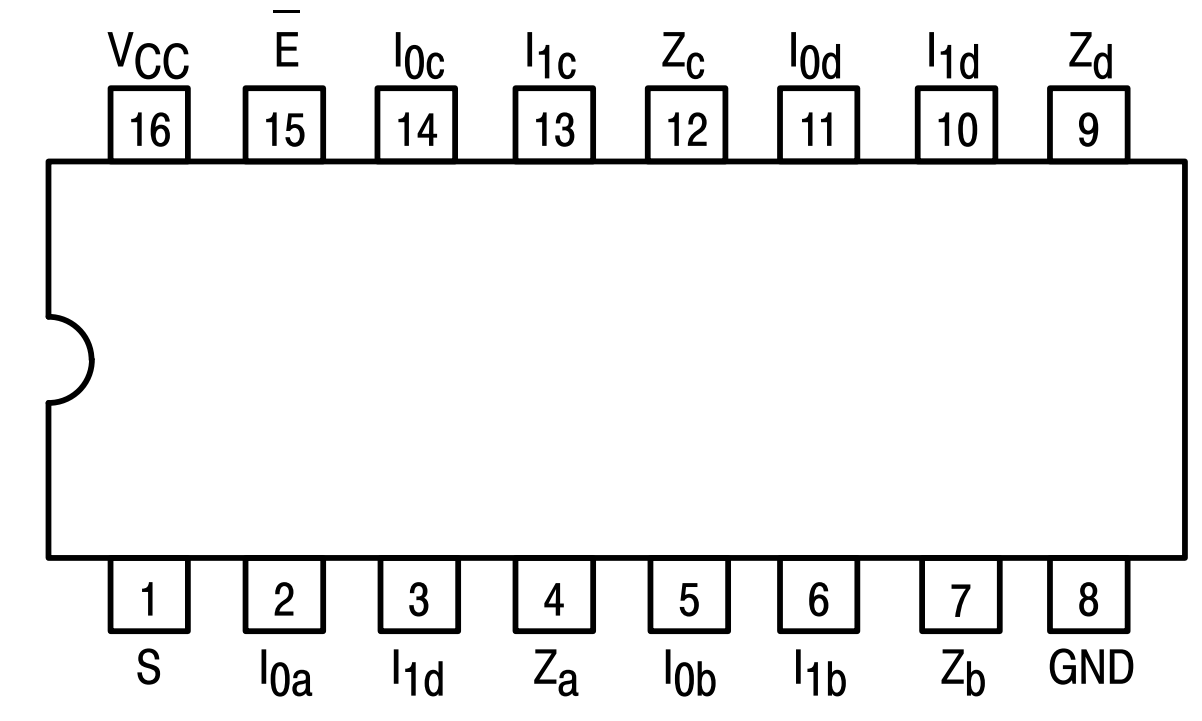
| 4 × 28C16 EEPROM | Double-throw toggle switch | 3 × Momentary tact switch |
| 8-position DIP switch | 4-position DIP switch | Slide switch |
| 100 × Assorted colour flat LED | 5V Power supply | 4 × Common Cathode 7-segment display |
| 10kΩ potentiometer | Arduino UNO | 24-pin ZIF socket |
| 2 × SMD 595 shift register | 2 × 74LS181 Arithmetic Logic Unit (ALU) | 12V Power Supply |
| DP-DT SMD slide switch |
Procedure
This project started by doing research on the required parts and sources for said parts. Ben Eater’s website and walkthroughs proved extremely useful in determining the parts required and what function they served. Finding the parts was more difficult. The RAM, flip-flop and EEPROM chips are no longer in production and are only sold by certain providers. Fortunately, future classes can still make the computer as most of the chips are still sold through websites like DigiKey.
A note on the design of this computer. The computer designed in this project uses a Von Neumann architecture where all the parts interface via the central bus. Alternatively, one can use the Harvard architecture where parts independently interface with each other.
.png)
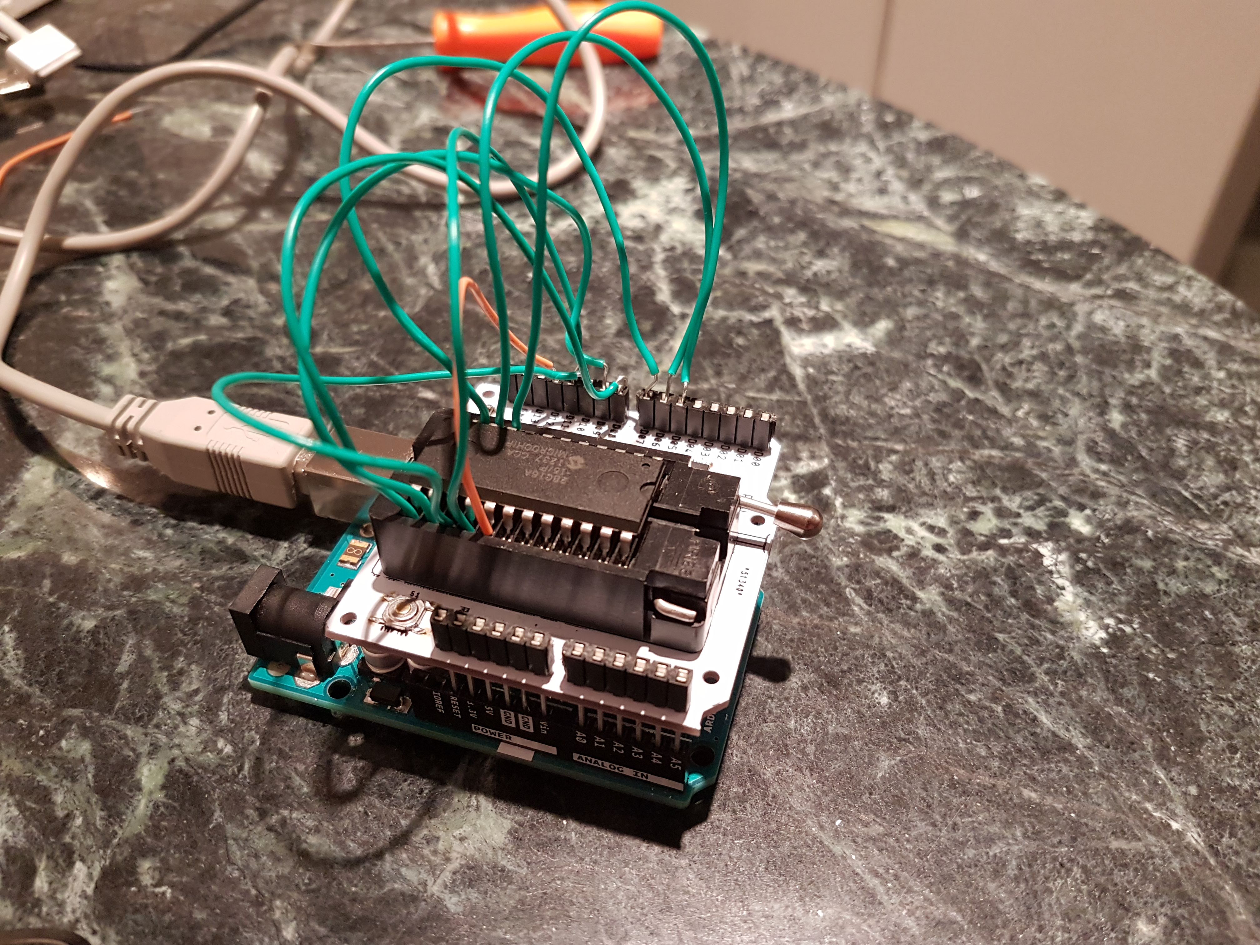
The next step was prototyping an EEPROM programmer. The initial design used a breadboard, two 595 shift-registers and Arduino UNO to interface with the EEPROM device. Digital pins 5 through 11 interfaced with the EEPROM directly via the data input/output pins. By connecting these pins to the Arduino, it is simpler to read back the data on the chip. The code can use a simple digitalRead() function instead of shifting in data from more 595 shift-registers. To write the data in the required positions, the code uses shift-registers to assign addresses during write/read cycles. The Chip Enable (CE) pin is also connected to the shift-registers. The Write Enable (WE) pin toggles low after the program sets the address and data pins to their requested values. This step is what tells the EEPROM to store the data into memory. This step proved especially difficult at the beginning of the year when the class worked on a 4-bit TTL computer. The solution to this problem was changing the EEPROM chip from a 28C17 to a 28C16A. Independent testing of the EEPROM chip with an 8-position DIP switch and LEDs ensured that the chip worked as intended.
The EEPROM programmer code used by Ben Eater in his project is the basis for this device. Fundamentally, there is only one way to program the EEPROM chip in this circuit. The code works by taking input in an array of name writeData[]. The code iterates through this array until each byte of EEPROM is set to the desired value. To save time the code writes only the required data to the EEPROM by assessing the size of writeData[] before programming. The writeEEPROM() function first uses the setAddress() function to assign which address to write to via the shift-registers. The code pulls high the Output Enable (OE) pin here too as required to write data. Next the program sets the required states of the data pins to reflect the selected byte of writeData[]. The WE pin momentarily toggles low for each byte to complete the write. The readEEPROM() function operates in much the same way except that the OE pin is low and digitalRead() replaces digitalWrite(). Also, the WE pin is not tripped.
Following this step was the designing of an EEPROM programmer Arduino shield. The advantage of using a shield is that EEPROM programming can be simple and quick. Furthermore, a 12V power supply can connect to the Arduino and the user can utilize the “Chip Clear” function to quickly wipe the data. The user simply slides a switch and clicks a button to overwrite the chip with ‘1’s. This switch applies 12V to the OE pin and the button grounds the WE pin. When the switch is in chip clear position a green LED illuminates. Unfortunately, the first iteration of this PCB had the data lines omitted and thus required jumper wires to properly program the chip. Version two seen here includes these wires.
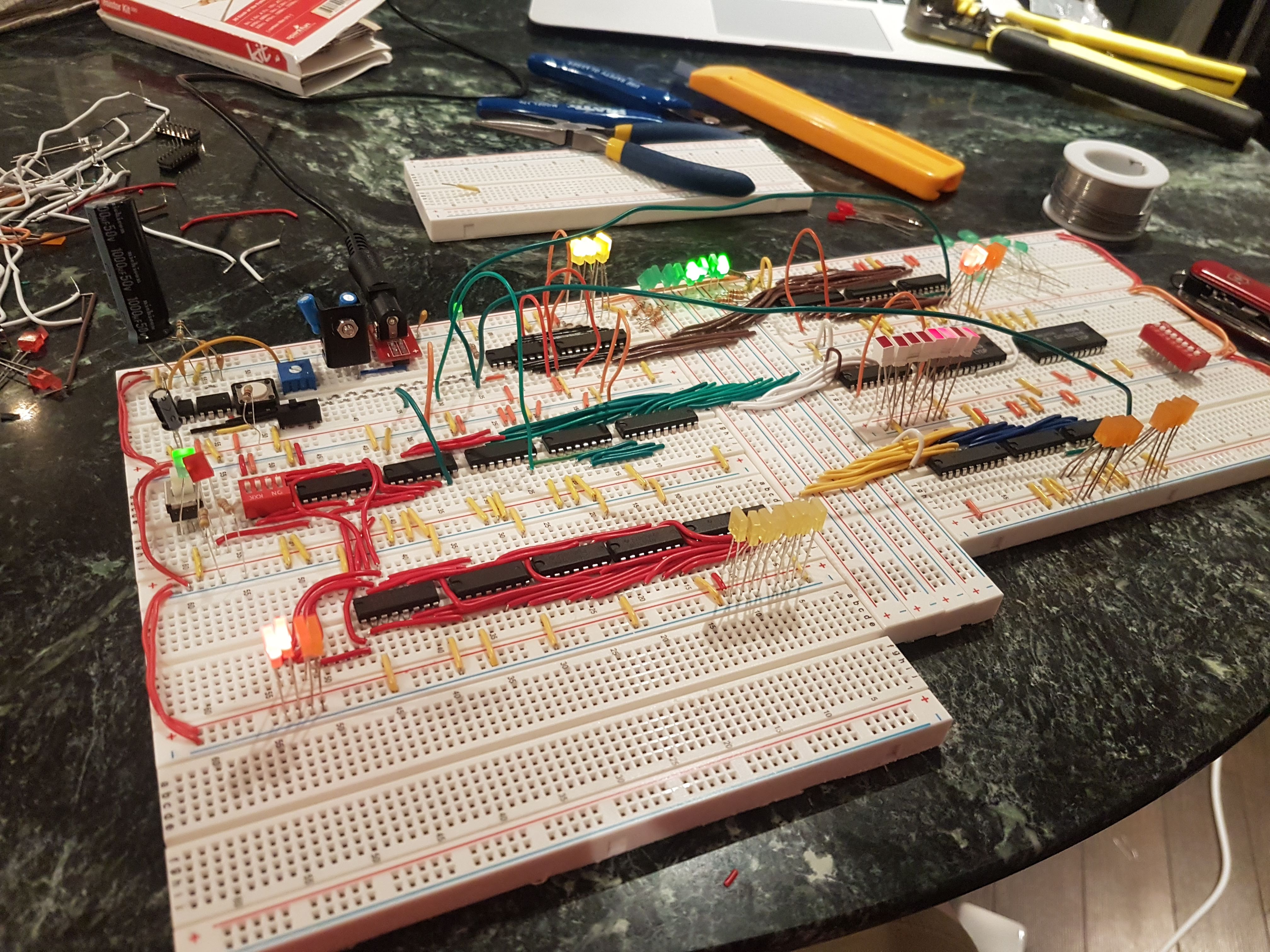
There was no idle time while waiting for the EEPROM programmer PCBs to arrive. The construction of the computer itself occupied this time and much more. The assembly of the computer took place in multiple steps correlating with the different modules.
The first step was the assembly of the clock module. This consists of two 555 timer ICs (as used in 555 Boost Converter). One of the timers operates in astable mode creating a constant, yet adjustable, pulse on its output. The other functions as a debouncer for the manual clock signal. A slide switch determines the source of the clock signal. The difficulties here were getting the clock to work in a reliable manner. Often it ran into problems where it would work fine at first and then cease to function properly.
Installing the program counter was the next step. The program counter consists of a 74LS161 4-bit synchronous binary counter and a 74LS245 Octal bus transceiver. The 74LS161 is the fundamental part of the counter, increasing as the clock pulse increases. The 74LS161 also take input from the 74LS245. In normal operation, this does not affect the function of the counter as the output from the 74LS245 matches the value on the 74LS161. However, if the code includes a JUMP function, the bus transceiver will have a different value on its input and the program counter will adjust its value accordingly.
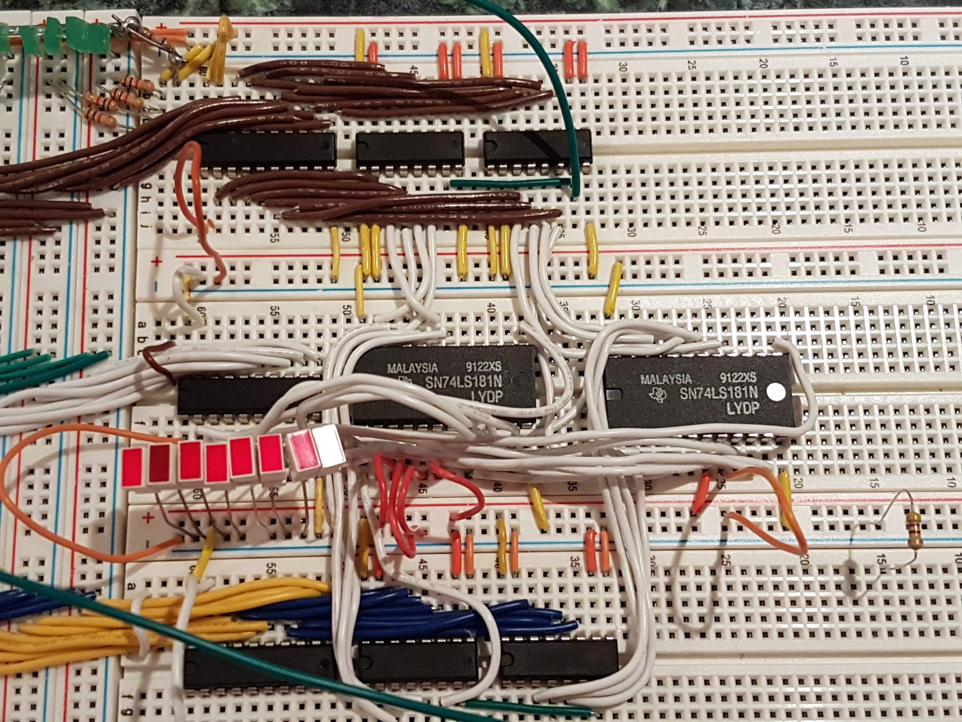
The next step was the construction of the registers. There are three registers in this computer, the A register, the B register and the Instruction Register (IR). The A and B registers are the inputs to the ALU. Each register can store an 8-bit value for one clock cycle. This means that each register can store a different value from the bus. Each register of the computer uses two 74LS173 4-bit D-type registers in combination to store these values. The instruction register is unique in that it interfaces with bus directly as well as with the instruction EEPROM and, by extension, the program counter. Because the IR is so closely linked to with the instructions, the first 4 bits do not connect to the bus and instead determine where in the EEPROM the computer is reading code from.
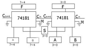
Following this is the installation of the ALU. The ALU is essentially the “brains” of the computer. Its function is to perform all of the arithmetic and logical operations that the user programs the computer to complete. By chaining two 74LS181 chips as shown, they can operate as a single 8-bit unit. Chaining works by connecting the carry+4 pin to the carry in pin of the upper nibble ALU. Connecting the select inputs (‘S’ pins) of each ALU to each other means that each chip is performing the same operation on the input values. By changing the values of the S pins, the operation of the ALU changes. The M pin determines whether the ALU is performing a logical or arithmetic operation. Arithmetic operations would include ADD, SUBTRACT, MULTIPLY, etc. Logical operations use Boolean logic and include NAND, XOR, NOT, etc. The ALU in this computer varies greatly from the computer in Ben Eater’s example. Instead of having merely 2 operations (ADD and SUBTRACT), this computer has a full set of ALU functions. The output pins (‘F’ pins) connect to the associated 74LS245 bus transceiver chip. From here the operation is complete and the result appears in the output section.
The final part of the computer assembled here is the Random-Access Memory (RAM). There are two settings for the RAM and three sub-modules that make up the whole module. The RAM can either be in program mode or read mode. A push button switch connected to red and green LEDs determines which mode the RAM is in. When the red LED is on, the computer is in program mode and it accepts input on the 4-position and 8-position DIP switches. The 4-position switch selects the address for the data and the 8-position switch is the data itself. To complete the write, the orange RAM IN pin must be high and the user must press the black momentary switch. The RAM is in read mode when the green LED is on. Here the RAM take input from the bus and outputs the value of the RAM at that address. These two modes work on the same RAM chips but use different sources for data. As such, the architecture uses the 74LS157 Quad 2-to-1 line data selector to determine which source the data should come from. This chip is also called a multiplexer. Both the switches and the bus connect to these chips and the select pins choose which of the inputs is sent to the output pins. Only the least significant nibble connects to the 74LS157 controlling the address. This is because only the address value is only ever 4 bits long (a limitation of the 4-bit program counter). Important to note is that the output of the RAM chips is active low. As a result, the chips require an inverter to connect to the bus transceiver. This is because the bus operates active high.
There are still a few modules missing from this computer. Most notably, the output and input registers are missing.
The output register operates on a programmed EEPROM that converts binary values on the bus to decimal numbers on 7-segment displays. This works by taking input from the bus and converting this binary value to the appropriate decimal number. The EEPROM, however, has only 8 outputs, enough for only one 7-segment display. The solution to this problem is POV (see BiColour LED Matrix). An external clock can count through the extra three address lines of the 28C16 EEPROM by using a 74LS76 Dual JK flip-flop. This flip-flop will count up to three (four different values) in binary. These two output wires connect to the EEPROM and a 74LS139 Dual 2-line to 4-line decoder, also known as a de-multiplexer. Connecting the two wires to the EEPROM can tell the chip to output the ones, tens or hundreds digit of the input address lines, as specified when programming the chip. The 74LS139 turns off one of its four output pins depending on the input of the two lines coming from the JK flip-flop. The computer can control each display independently by connecting the four outputs of the 74LS139 to the common cathode of the 7-segment displays Each time one of the pins is at 0V, the associated display turns on. With a high enough clock cycle, it is impossible to tell that only one display is on at any given time.
The input module also uses an EEPROM chip. The program counter addresses each input of the EEPROM and the 8 output pins address the appropriate control signals. There are, however, many more control signals in this build than anticipated due to the complete ALUs. The completed design will require multiplexers and de-multiplexers to address the full suite of control pins.
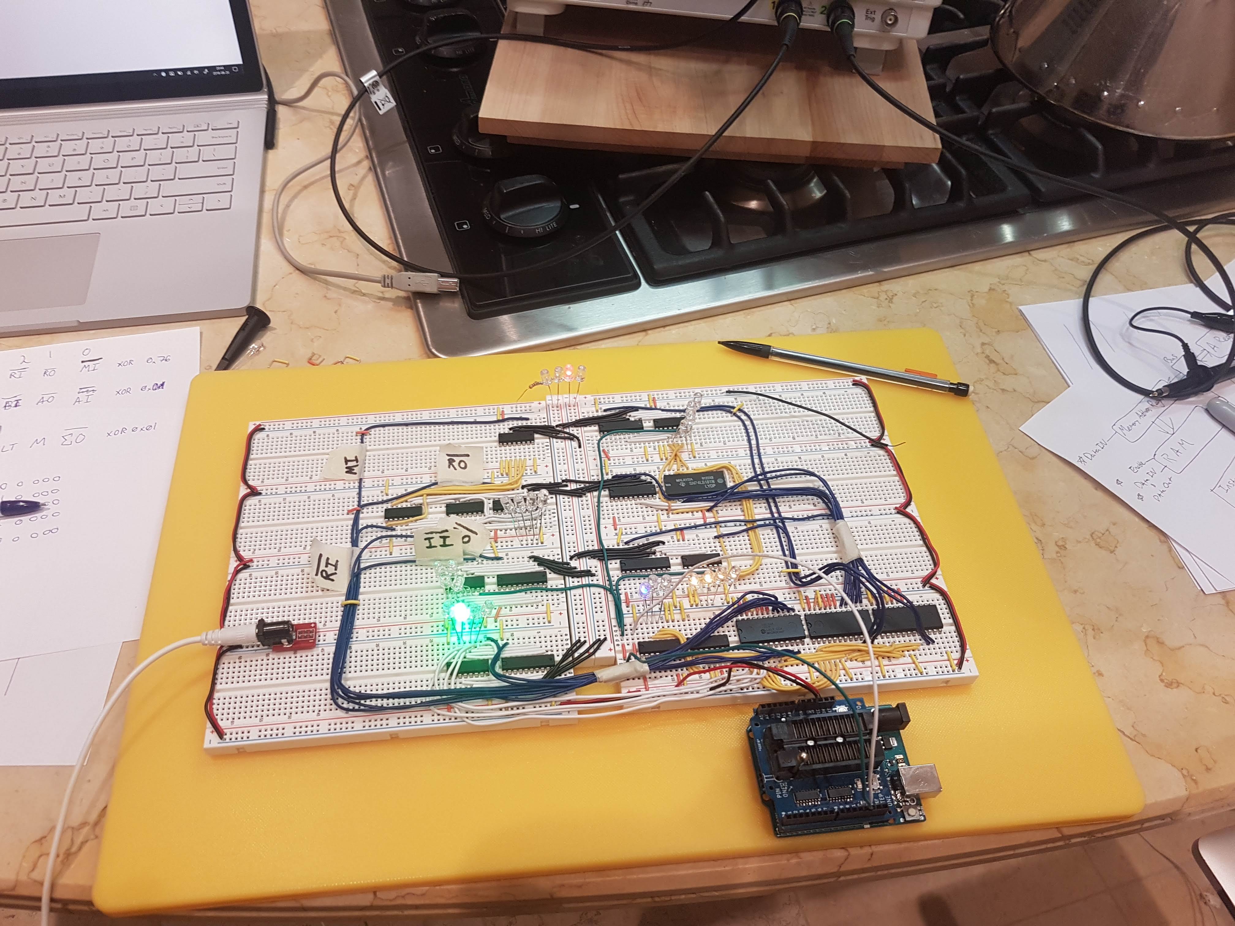
Media
 |  |
| RAM module and IR register | EEPROM Programmer Shield (Version 1) |
|---|---|
 |  |
| ALU (middle) with A (top) and B (bottom) registers | The computer mid-way through RAM construction |
| Link to YouTube Video: https://youtu.be/aaMhVgkE8aw | |
Code
EEPROM Programmer
#define DATA 2
#define CLOCK 3
#define LATCH 4
#define D0 5
#define D7 12
#define WE 13

uint8_t writeData[] = {0x00, 0x01, 0x02, 0x03, 0x04, 0x05, 0x06, 0x07, 0x08, 0x09, 0x0a, 0x0b, 0x0c, 0x0d, 0x0e, 0x0f};

void setup() {
  Serial.begin(9600);

  pinMode(DATA, OUTPUT);
  pinMode(CLOCK, OUTPUT);
  pinMode(LATCH, OUTPUT);
  pinMode(WE, OUTPUT);

  digitalWrite(WE, HIGH); //WE is active low

  Serial.print("Programming");
  for (int address = 0; address < sizeof(writeData); address++) {
    writeEEPROM(address, writeData[address]);

    if (address % 64 == 0) {
      Serial.print(".");
    }
  }
  Serial.println(" done");

  Serial.println("Data:");
  printContents();
}


void loop() {
  printContents();
  delay(10000);
}


void setAddress(int address, bool outputEnable) {
  shiftOut(DATA, CLOCK, MSBFIRST, (address >> 8) | (outputEnable ? 0x00 : 0x80));
  shiftOut(DATA, CLOCK, MSBFIRST, address);

  digitalWrite(LATCH, LOW);
  digitalWrite(LATCH, HIGH);
  digitalWrite(LATCH, LOW);
}

byte readEEPROM(int address) {
  for (int pin = D0; pin <= D7; pin++) {
    pinMode(pin, INPUT);
  }
  setAddress(address, true); //output enable on for read

  byte dataIn = 0;
  for (int pin = D7; pin >= D0; pin -= 1) {
    dataIn = (dataIn << 1) + digitalRead(pin);
  }
  return dataIn;
}

void writeEEPROM(int address, byte inByte) {
  setAddress(address, false); //output enable off for write
  for (int pin = D0; pin <= D7; pin++) {
    pinMode(pin, OUTPUT);
  }

  for (int pin = D0; pin <= D7; pin++) {
    digitalWrite(pin, inByte & 1);
    inByte = inByte >> 1;
  }
  digitalWrite(WE, LOW);
  digitalWrite(WE, HIGH);
}

void printContents() {
  for (int base = 0; base <= 255; base += 16) {
    byte readData[16]; //28C16 has 16k (2^14) of memory with 2^11 adresses but the computer can only address 2^8
    for (int offset = 0; offset <= 15; offset++) {
      readData[offset] = readEEPROM(base + offset);
    }

    char buf[80];
    sprintf(buf, "%03x:  %02x %02x %02x %02x %02x %02x %02x %02x   %02x %02x %02x %02x %02x %02x %02x %02x",
            base, readData[0], readData[1], readData[2], readData[3], readData[4], readData[5], readData[6], readData[7],
            readData[8], readData[9], readData[10], readData[11], readData[12], readData[13], readData[14], readData[15]);

    Serial.println(buf);
  }
}
Conclusion
This was an extremely difficult and extraordinarily time-consuming project. I do not regret taking on the challenge of a completely functional computer, however I do regret pursuing one of this level of difficulty. That is to say that I should have chosen a much easier architecture or simply created a 4-bit computer instead of an 8-bit. In hind sight, it would have been a much better idea to simply adapt the 4-bit TTL computer we made in class to operate on the 28C16 EEPROM. I do not want to stop working on this project, however. I would like to continue to develop the computer until it is complete. I believe that either a complete 8-bit version on a PCB or a smaller 4-bit breadboard version of this computer would prove extremely useful to future generations of ACES. I found the TTL computer project at the beginning extremely fun and informative even though it never worked. Despite the amount of time I have invested in this project and its less than perfect result, I am satisfied. Hopefully my newfound knowledge will prove useful in university and beyond. I am glad to have been a part of this truly amazing ACES program. I think that this project is an excellent way to end an outstanding three years.
Reference
D'Arcy, Chris. “TEI4M Major Project: The Computer.” ICS4U Software Engineering Tasks, RSGC ACES, 8 Sept. 2017, http://darcy.rsgc.on.ca/ACES/TEI4M/4BitComputer/index.html.
Eater, Ben. “Build an 8-Bit Computer from Scratch.” Ben Eater, 18 Apr. 2017, https://eater.net/.
Update
This summer (2018) I successfully built a 4-bit variation of this computer. I've got some photos below.
 |  |
| New EEPROM programmer board (fully operational) | Populated board |
|---|---|
 |  |
| Computer in operation | Top-Down view showing the parts a little better |